- Factory-Direct Pricing | No Middleman Markups
- Save 30%-My Sourcing
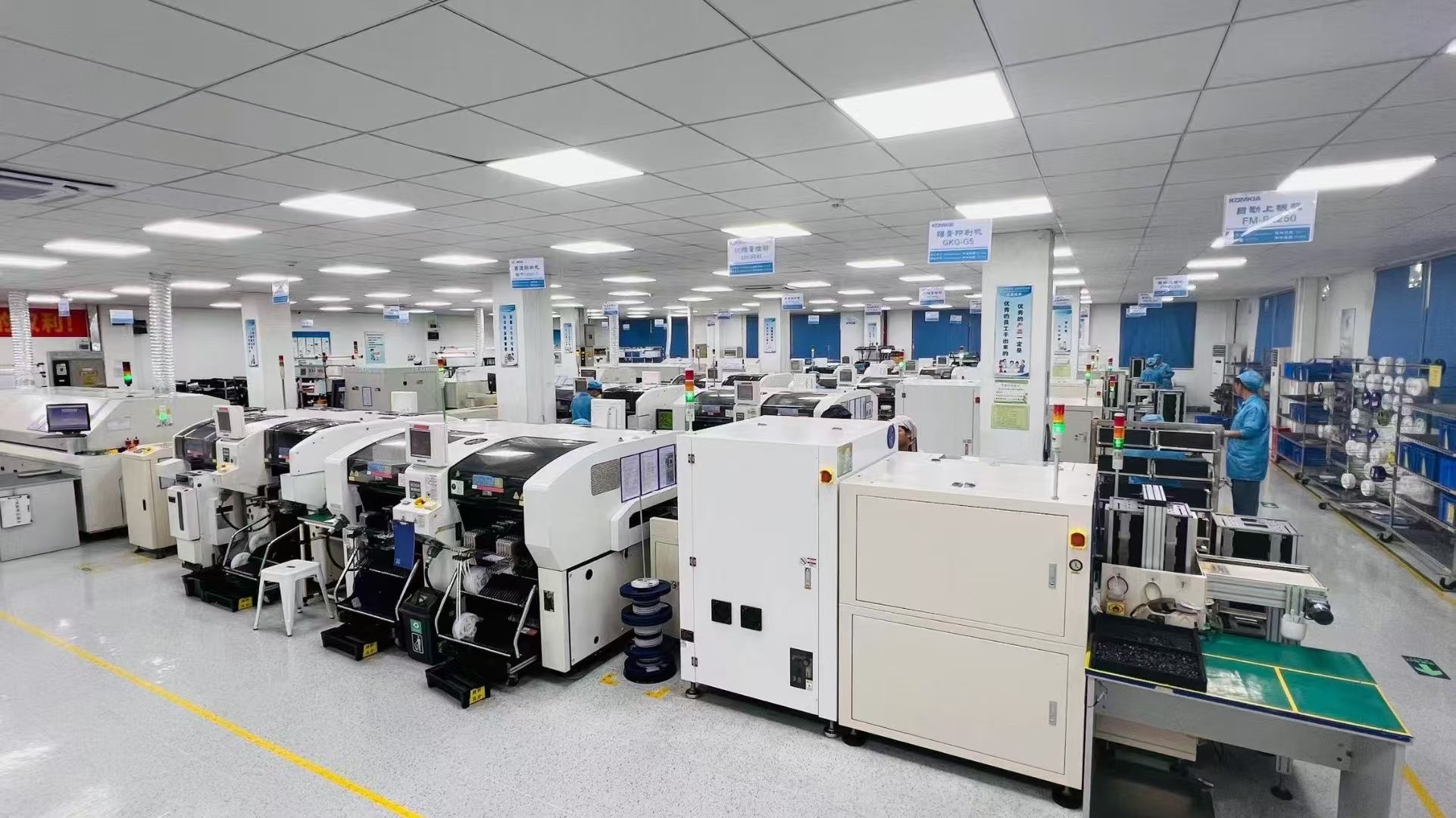 printed circuit board assembly manufacturer
Overpaying for printed circuit board assembly sourcing? Hire me to connect with PCB assembly factory-direct, cut out 30% costs! From Gerber files to delivery: DFX/DFM/QC support, optimizing layout, BOM parts sourcing, Let’s talk now!
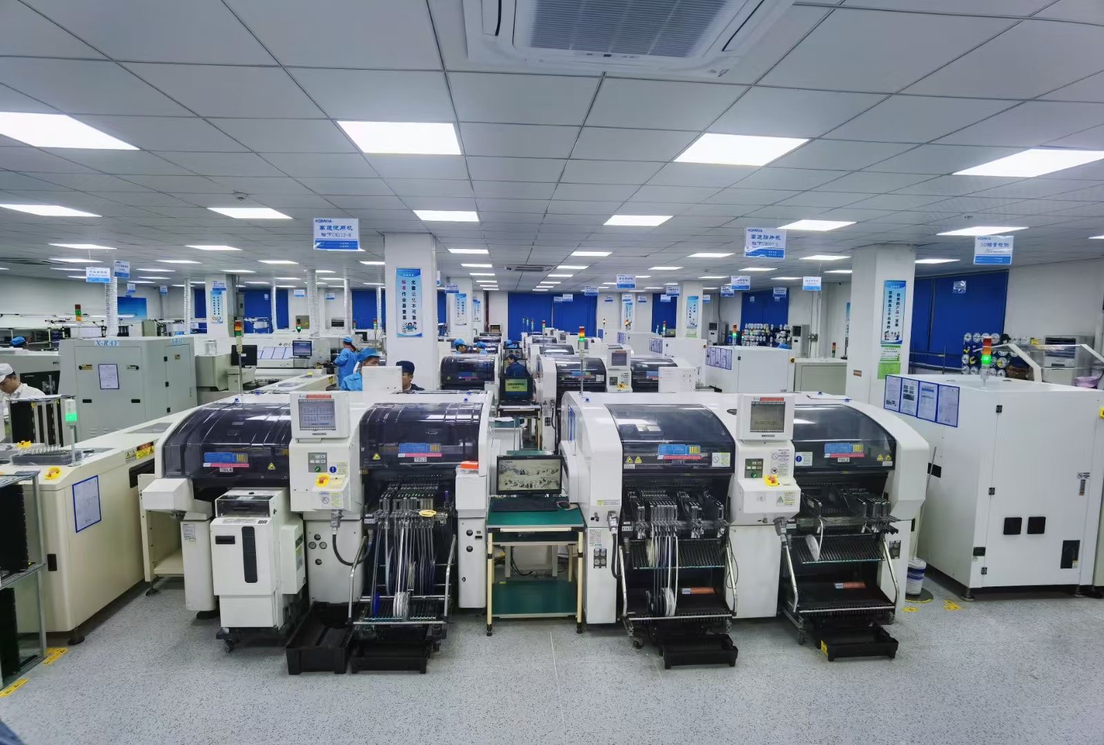
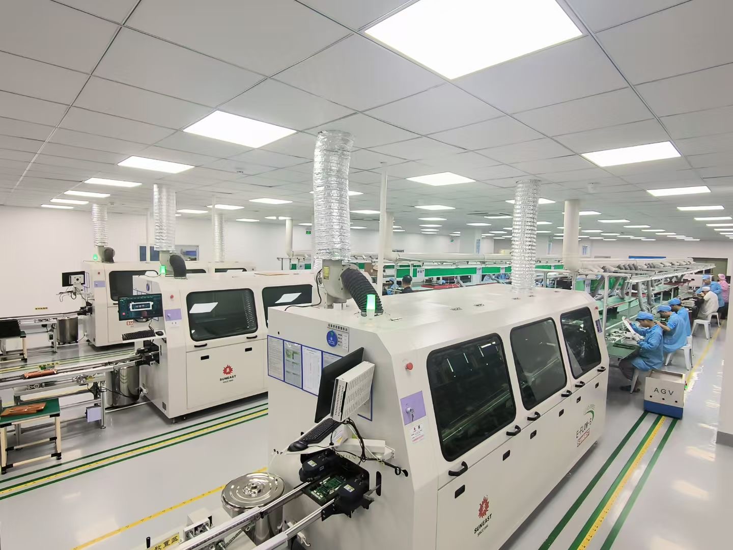
Printed Circuit Board Assembly Sourcing Service | Design Review, Optimized BOM, Smart Component Sourcing. Full Traceability, Low MOQ, Cut 30% Production Costs Today!
SMT (Surface Mount Technology), also known as SMD (Surface Mount Device), is a crucial method in modern electronics manufacturing where components are directly mounted onto the surface of printed circuit boards (PCBs). This technique offers multiple benefits, including higher component density, improved vibration resistance, and reduced production costs compared to traditional through-hole components. The utilization of SMT enables the creation of smaller and lighter electronic devices, making it a popular choice in various industries such as consumer electronics, automotive, and healthcare. Engineers and manufacturers often prefer SMT due to its efficiency in mass production and its compatibility with automated assembly processes. Understanding the intricacies of SMT, including component placement, soldering techniques, and quality control measures, is essential for ensuring reliable and high-performance electronic products. Overall, SMT plays a vital role in enabling the advancement of technology and innovation by providing a streamlined and effective approach to electronic manufacturing.
In the dynamic world of electronics manufacturing, innovation, precision, and reliability are paramount. As a leading OEM (Original Equipment Manufacturer) and ODM (Original Design Manufacturer) factory, we specialize in delivering end-to-end PCB Assembly and Printed Circuit Board Fabrication services tailored to meet the diverse needs of international clients. From concept to mass production, our mission is to empower your innovations with cutting-edge technology, unwavering quality, and a customer-centric approach.
Why Partner with Us?
With decades of expertise, we bridge the gap between design and delivery, offering scalable solutions for industries ranging from automotive and aerospace to medical devices and IoT. Our global footprint, combined with localized support, ensures seamless collaboration across time zones and markets.
Comprehensive PCB Assembly Services
We transform your designs into high-performance electronic assemblies with state-of-the-art technology:
1. Advanced Assembly Techniques:
– SMT (Surface-Mount Technology)**: High-speed automated lines for precision placement of micro-components.
– THT (Through-Hole Technology): Robust solutions for components requiring mechanical stability.
– Mixed Technology & Complex Assemblies: Expertise in BGA, QFN, and micro-BGA for high-density designs.
2. Quality Assurance:
– Automated Optical Inspection (AOI) and X-Ray Testing to detect defects invisible to the naked eye.
– In-Circuit Testing (ICT) and Functional Testing to ensure 100% performance compliance.
3. Rapid Prototyping: Accelerate your R&D cycle with 24-hour turnaround prototypes.
End-to-End PCB Fabrication Capabilities
From simple single-layer boards to complex multi-layer architectures, our fabrication services include:
– Material Diversity: FR-4, Rogers, Polyimide, and flexible/rigid-flex options.
– High-Density Interconnect (HDI): Micro-vias and fine-pitch traces for compact, high-speed applications.
– Lead Time Flexibility: Express options for urgent projects without compromising quality.
OEM & ODM Solutions: Customization at Its Core
– OEM Services: Bring your designs to life with our precision manufacturing, adhering to your exact specifications.
– ODM Expertise: Leverage our R&D team for custom solutions—from concept development to certification-ready products.
– Industry-Specific Compliance: Designs optimized for ISO, IATF 16949 (automotive), ISO 13485 (medical), and more.
Global Supply Chain Mastery
Navigate component shortages and logistical challenges with our:
– Strategic Sourcing Network: Partnerships with Tier-1 suppliers to secure genuine components.
– Inventory Management: Safety stock programs and real-time tracking for risk mitigation.
– Logistics Integration: Door-to-door delivery with expertise in customs clearance and global shipping.
Sustainability & Compliance
We prioritize eco-conscious manufacturing:
– RoHS & REACH Compliance: Lead-free and hazardous substance-free processes.
– Waste Reduction: Energy-efficient facilities and recycling initiatives.
Dedicated Customer Success
– Multilingual Project Management: Seamless communication in English, Mandarin, German, and more.
– Transparent Collaboration: Real-time updates via ERP portals and weekly progress reports.
– After-Sales Support: Comprehensive warranty services and troubleshooting assistance.
Innovate Without Boundaries
In a world where technology evolves daily, partnering with a forward-thinking OEM/ODM factory is crucial. Whether you’re a startup prototyping a breakthrough idea or an enterprise scaling production, we provide the technical prowess, global agility, and unwavering quality to elevate your products.
Contact us today to discuss your project. Let’s turn your vision into a market-ready reality—efficiently, reliably, and innovatively. Crafted for clarity and impact, this article positions your factory as a holistic partner, blending technical depth with a commitment to global customer success.
My consulting services for PCB assembly can be tailored to provide solutions that are designed specifically for your business, whether it’s optimizing for suppliers development, BOM cost, quality, technology, delivery or a combination of these factors.
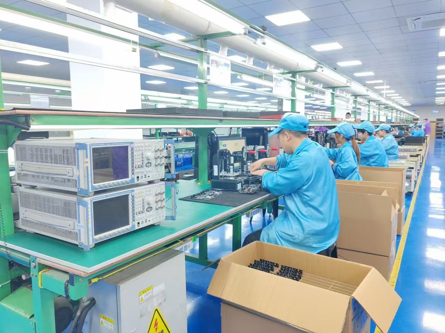
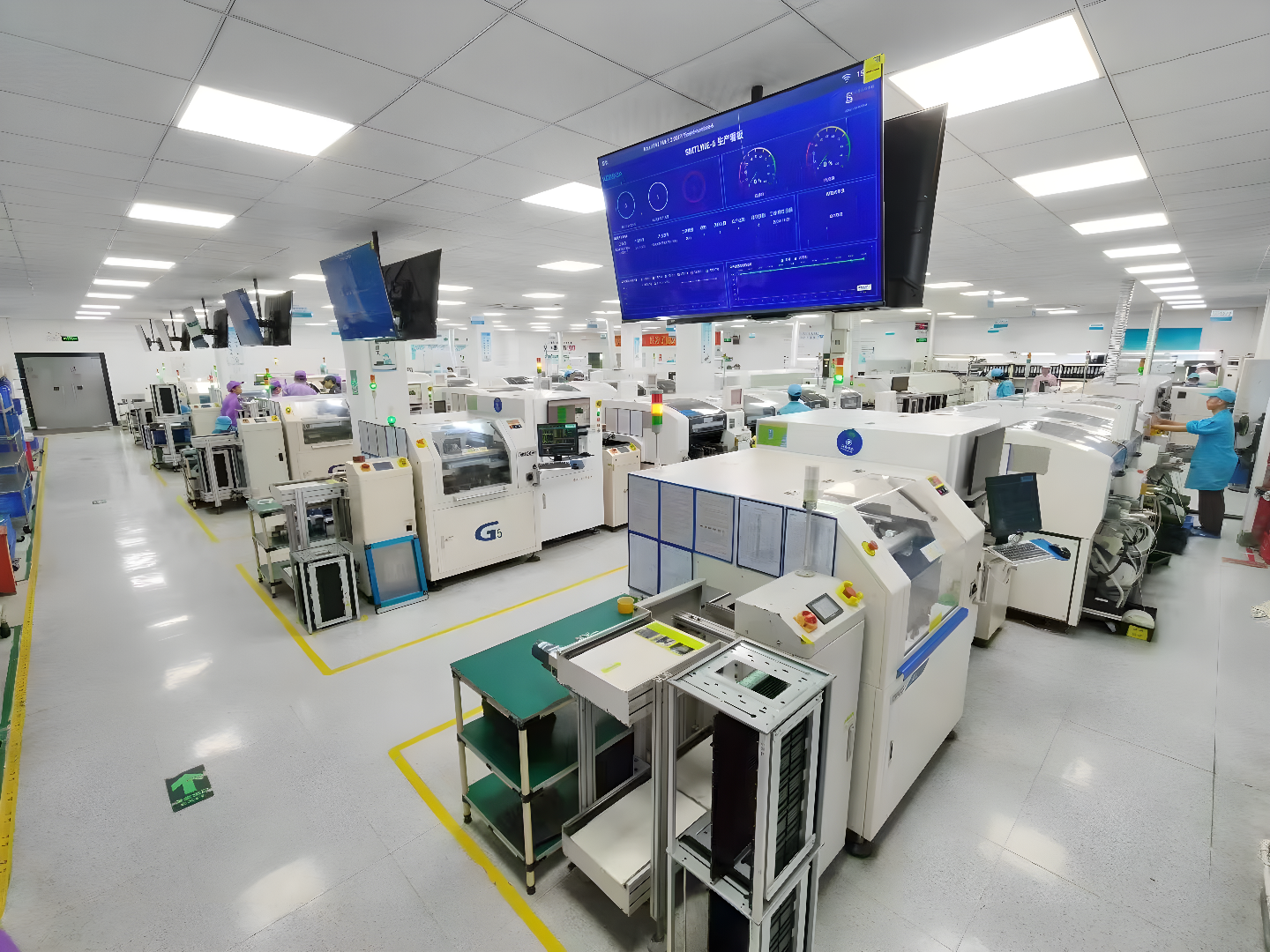
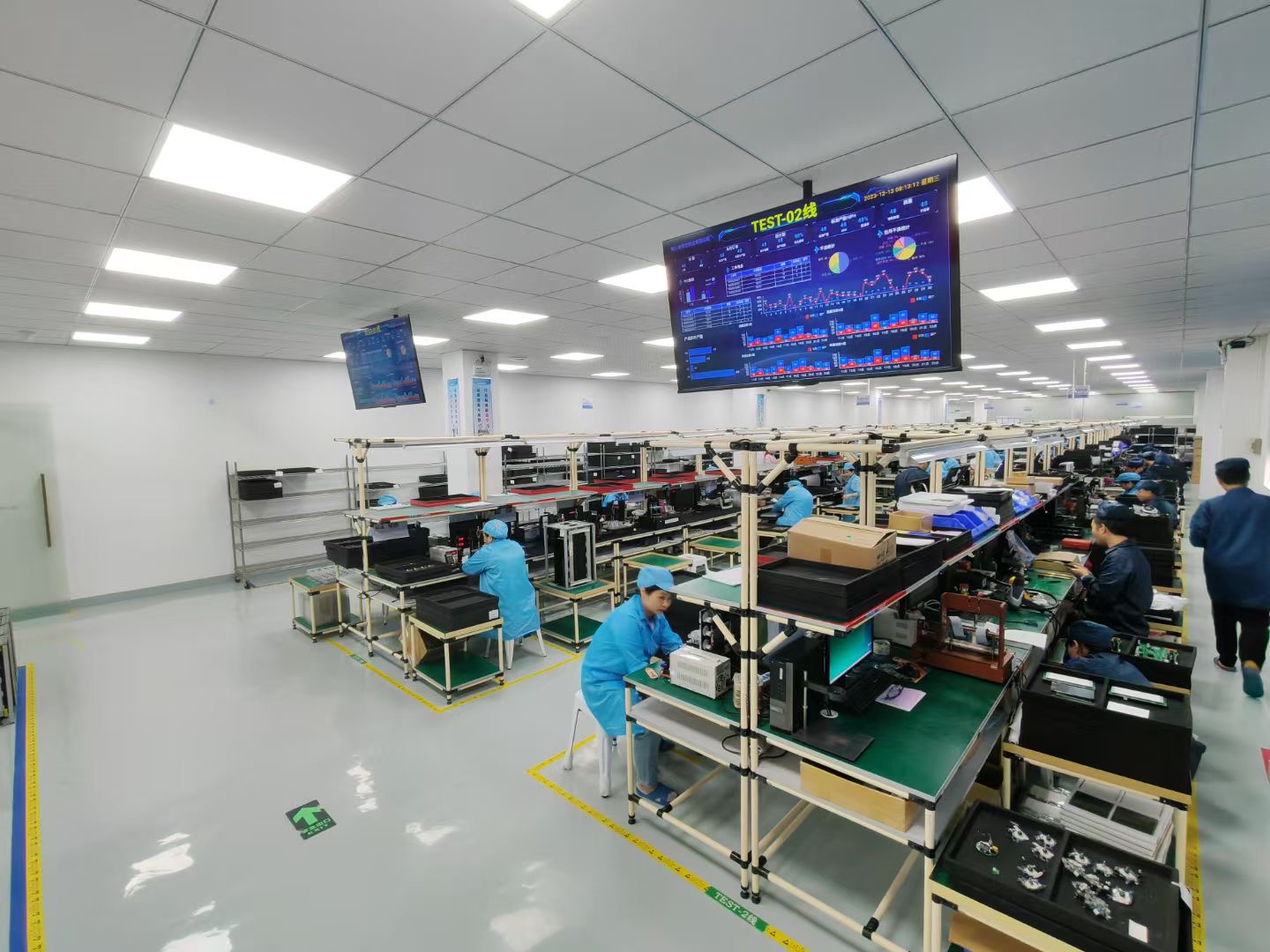
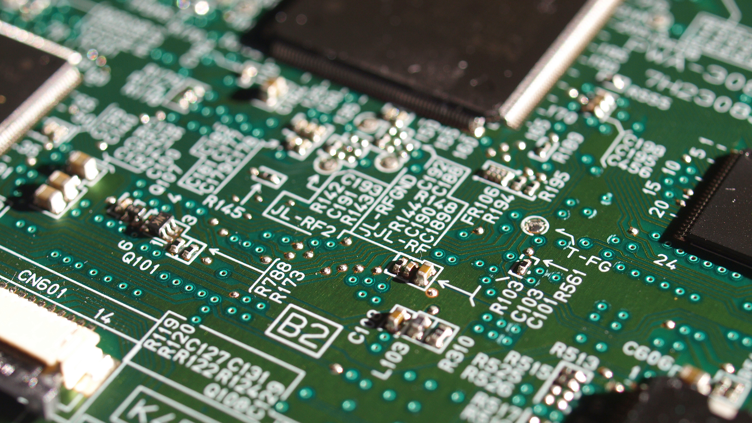
Automated Optical Inspection (AOI) testing is very common in the SMT industry and is suitable for all board production and PCB assembly. It is mainly used to judge the welding problems of components by the appearance characteristics of components. It can also be determined by checking the color and screen printing of the components on the IC, and whether the components on the circuit board are misaligned
FAI mainly is to do the first article PCBA through the integration of BOM table, coordinates and high-definition scanning of the first image automatic generation detection program, fast and accurate component detection, and automatically determine the result, generate the first article report. To achieve the purpose of improving production efficiency and capacity, while strengthening quality control.
DIP inspection is mainly inspect the bottom of the board, board surface, copper foil PCB circuit, through hole, etc., should have no cracks or cuts, no short circuit caused by bad cutting. The edge damage is acceptable within a certain length, more than the requirement is bad, bending degree is calculated based on the bending distance. Dip inspection ensure DIP processing compliance with quality standard.
X-RAY has strong penetration, and its perspective can show the thickness, shape and mass density distribution of the solder joint, which can fully reflect the welding quality of the solder joint, such as open circuit, short circuit, holes, bubbles inside the hole and insufficient tin and other quality problems.
ICT (In-circuit test) is contacted test technology, mainly used to mainly check out the failure problem includes bridge connection, false soldering, short circuit, open circuit, as well as the error such as component polarity and variety was mis-mounted, value overruns, etc.
FCT (Functional Circuit Test): PCBA power-up test, mainly including voltage, current, power, power factor, frequency, duty cycle, brightness and color, character recognition, sound recognition, temperature, pressure measurement, motion control, FLASH and EEPROM programing and other test items.
We offer our customers with free DFM checking: signal and mixing layer, power and grounding, drilling, soldermask and silkscreen analysis and checking, to ensure every detail is correct, and our engineers send engineering enquiries to our customers when they find any information that does not match with the original file or SMT process.
SPI is mainly used to check the quality of solder paste printing. It accurately measures and analyses the solder paste printed on the PCB by means of a high-precision camera and advanced image processing technology, including key parameters such as the height, volume, area, shape and position of the solder paste.
Steel surface tension standard in IPC electronic acceptance requirements contain reference indicators. The general use of steel mesh tension tester, placed at a distance of 15-20cm from the pitch, select 5-8 points, each square centimeter of tension is greater than 35 ~ 50 N. Ensure that the test results meet the specifications of the product.
+8619872870689
kinfomtech
No.1 Road East Hongfu, Dongcheng, Donguan, China.
+8619872870689
“From raw materials to retail-ready goods—we’re your all-in-one solution. Let’s optimize your chain!”